
Some time has passed since my last update on my Z80 computer and a lot of things have changed. First, I summarize some specs from the past posts and will not go deeply into details here. You can find more details here: Z80 Single Board Computer, Z80 work in progress.
- MCU: Z80 (Z8400B) at 7.3728 MHz, NMOS version for no real reason, CMOS would also be ok
- RAM: 628128 SRAM (128k available with bank switching, see text)
- ROM: AT28C64 EEPROM, AT28C256 possible (see text)
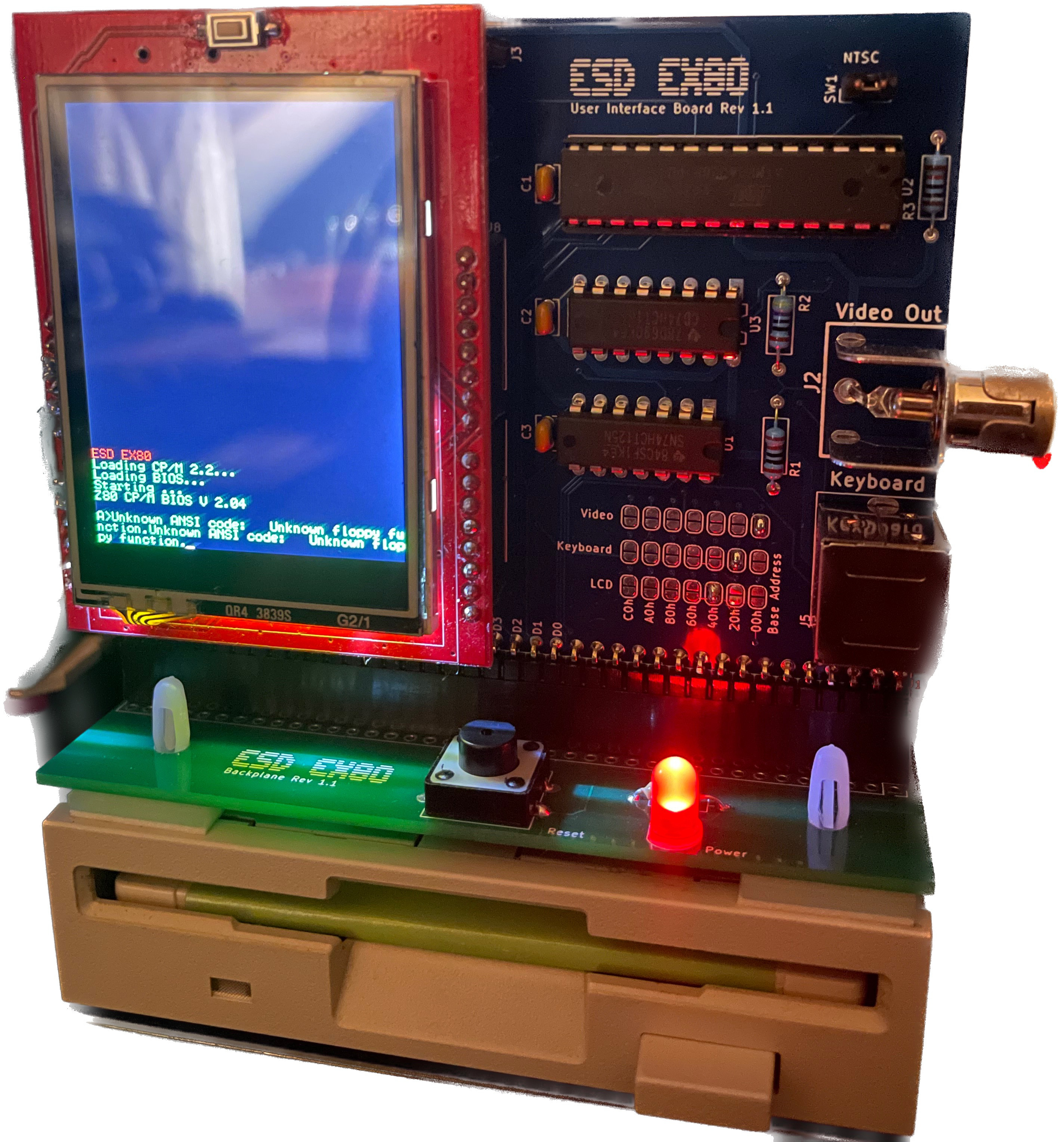
- Internal display: 320×240 TFT with ILI9325 controller
- External video (b/w), 80×25 characters
- PS/2 Keyboard
- 1.44 MB floppy disk, compatible with normal PCs
- CP/M 2.2
The overall system consists of at least 4 boards that are required to work: Mainboard, User I/O board, Floppy Controller and Backplane. The system and especially the bus is not compatible with RC2014, more about the bus in the backplane section. Some images show the old versions of the boards (see links above). The new PCBs were designed with KiCad 7 and produced by JLCPCB. Before I described everything, I give download links for everything that is required to build the system.
Note that this is not a commercial product or a well maintained software repo like RomWBW, so if you would like to write this firmware to your EX80 clone, you will have to adapt some things to your needs. See readme.md for details about the build procedure.
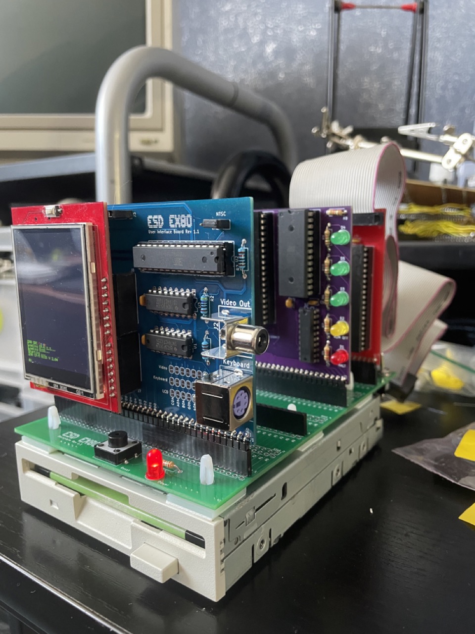
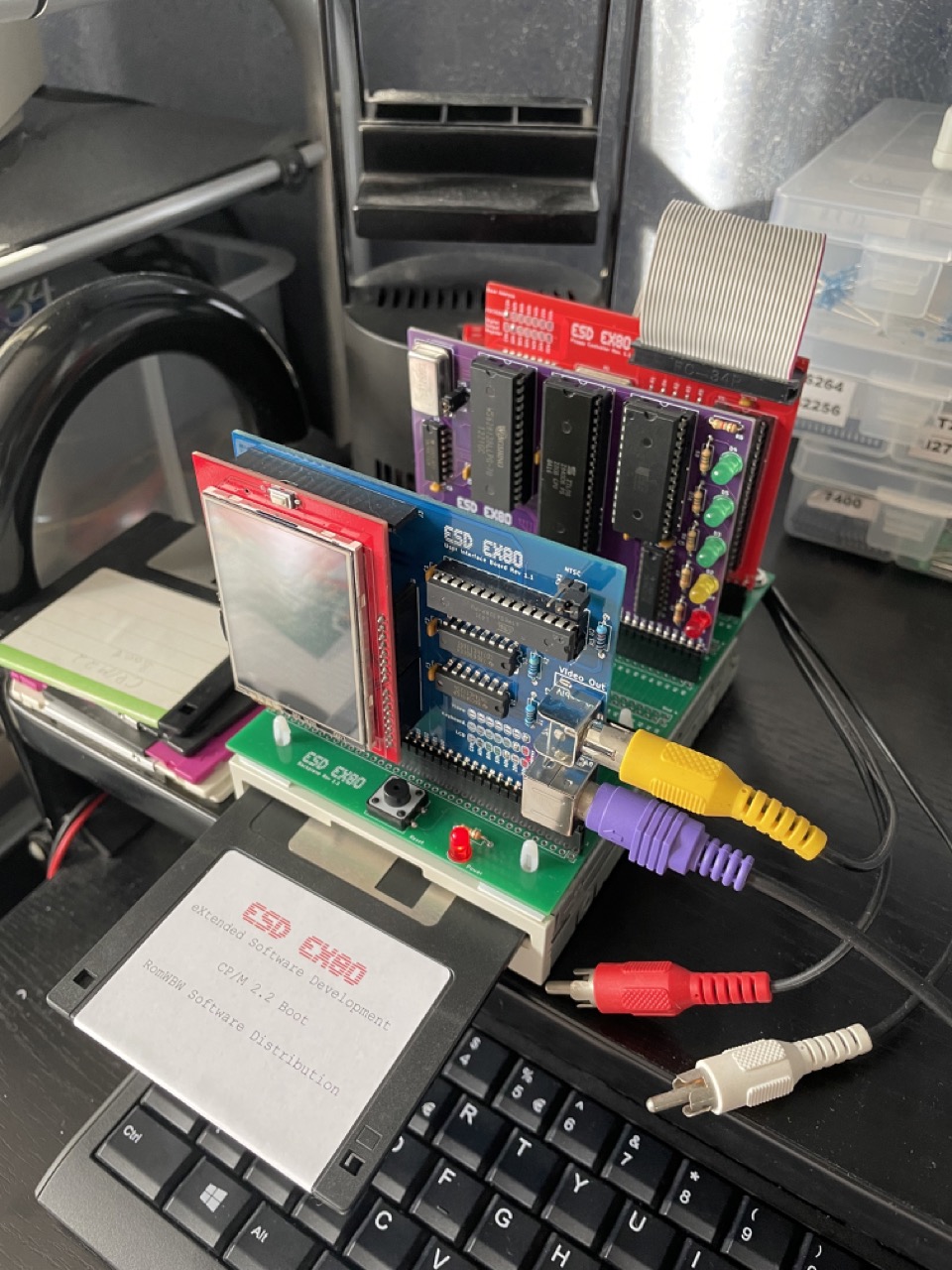
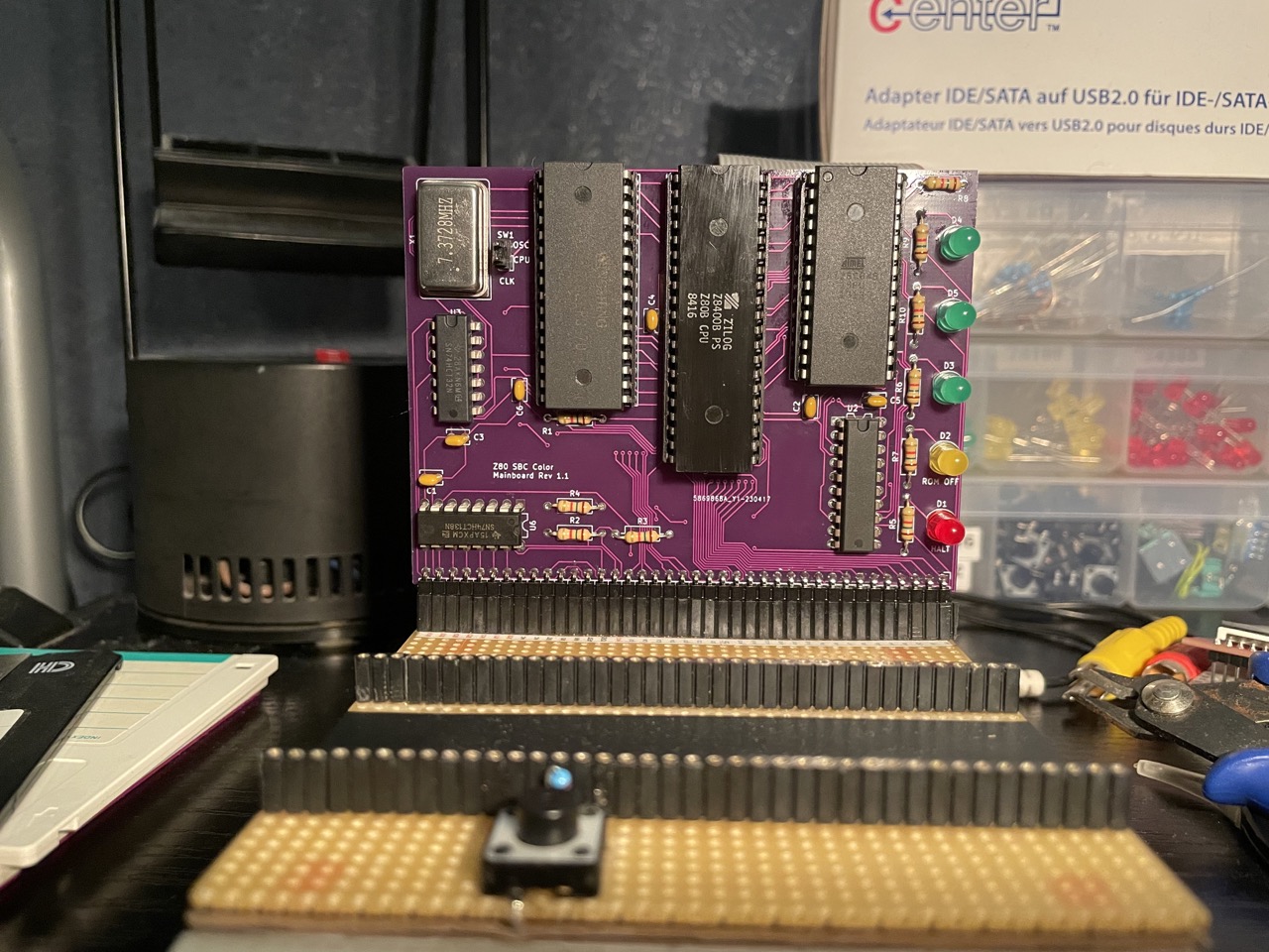
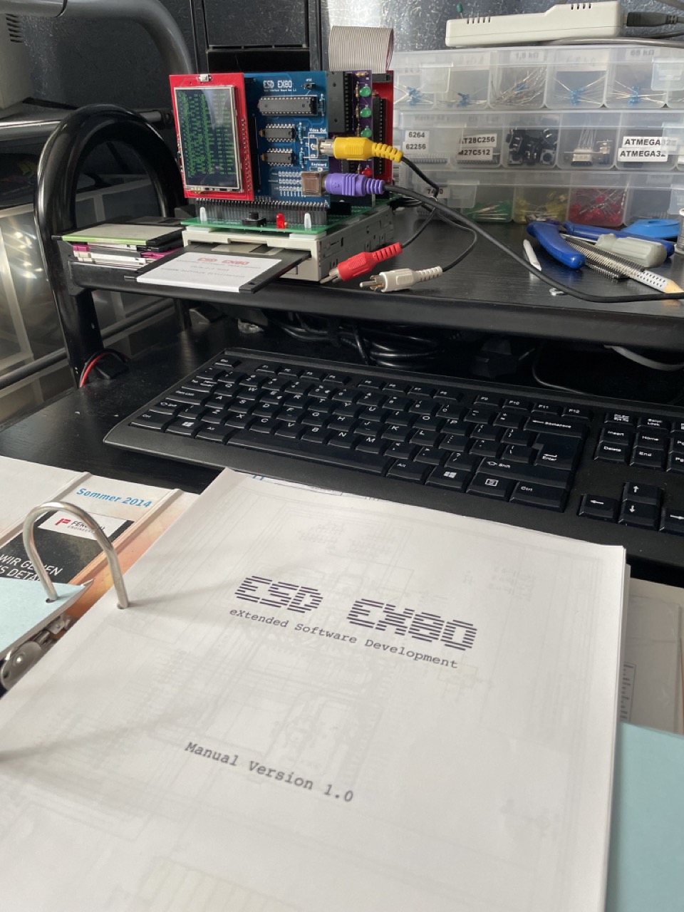
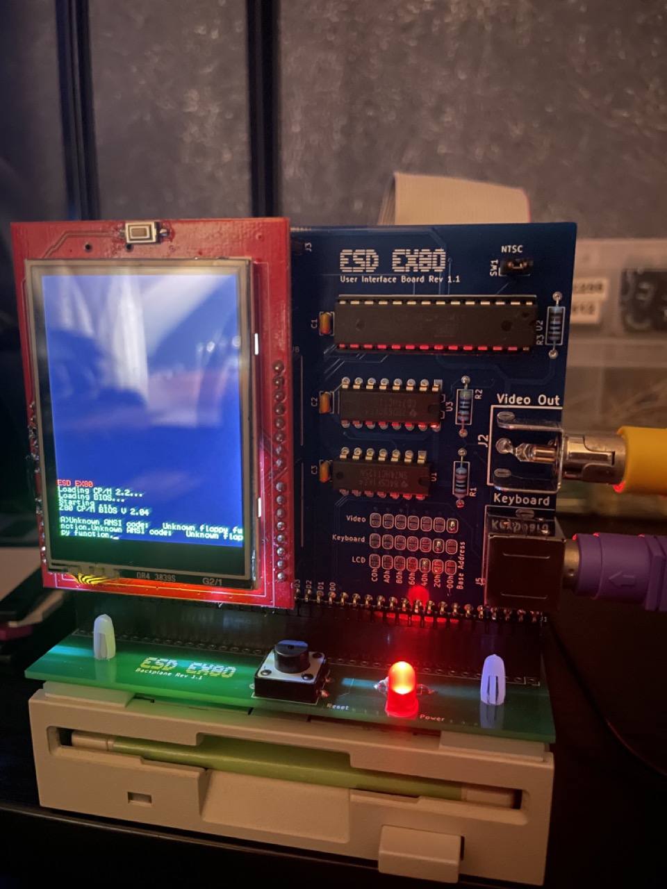
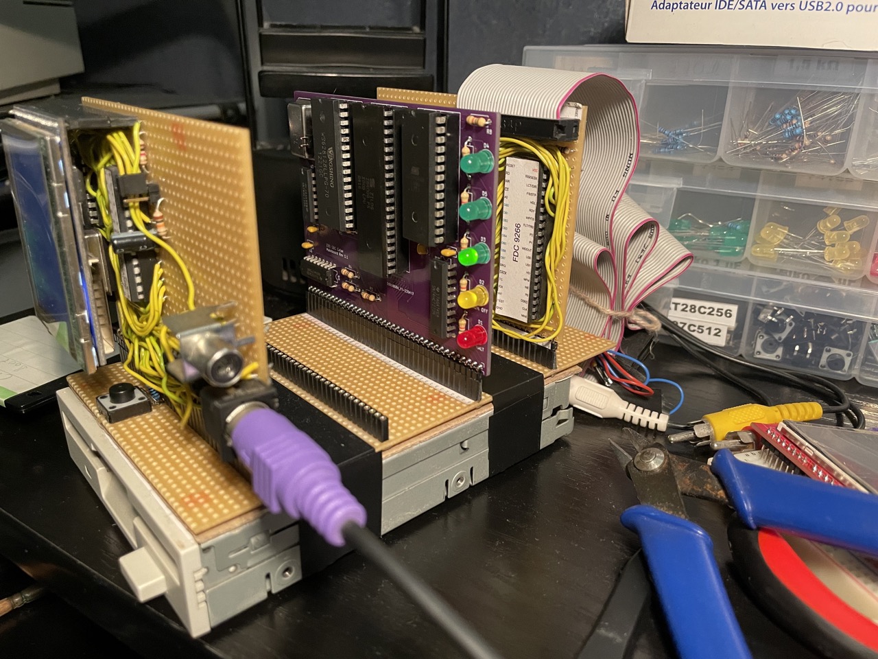
Table of Contents
Mainboard
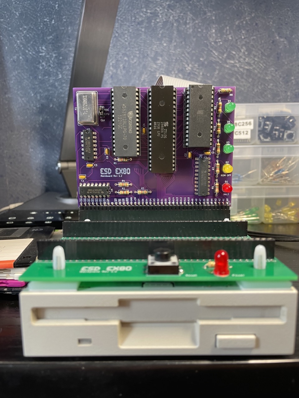
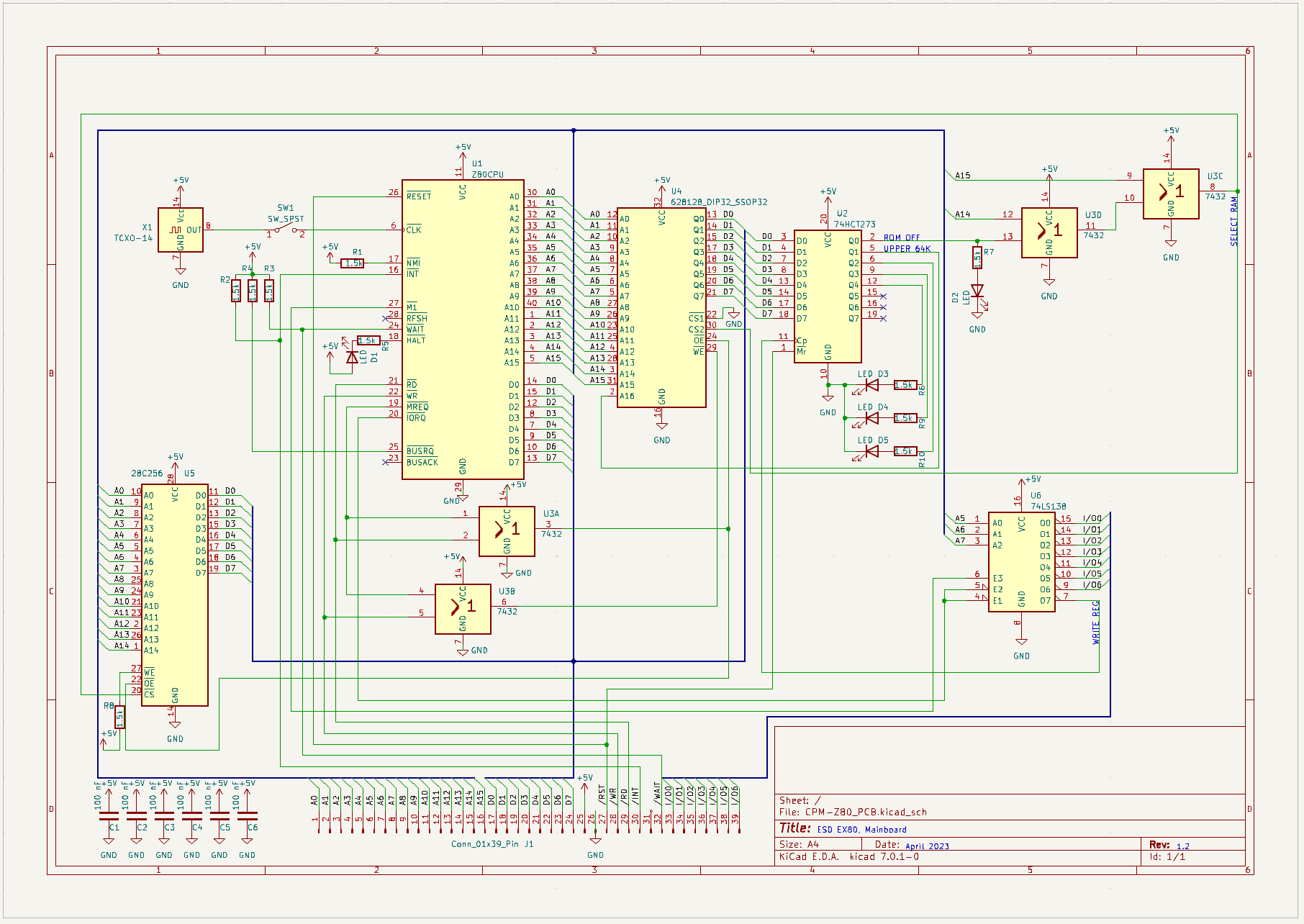
The mainboard is based on Grant’s design with a few changes. Like in his design, bit 0 of a 74HCT273 controls if the lower 16k are mapped to the ROM. As there are only 8k oder 32k EEPROMS, it currently has a 8 kb. It can be equipped with a 628128 SRAM und then has 128 kb RAM. The same register as above can select upper or lower 64k with bit 1. The other bits are for the green LEDs, while the yellow is wired to the ROM on/off bit and the red LED to HALT.
The clock of 7.73 MHz is connected via a jumper. Thus, in case you want a slower clock for software debugging, you could add a switch or microcontroller as clock generator and then watch the bus.
Differing from most designs, a 74HCT38 is on this board for I/O control. The I/O request number is thus not binary encoded on the bus, which simplifies the design of the other boards.
User I/O Board

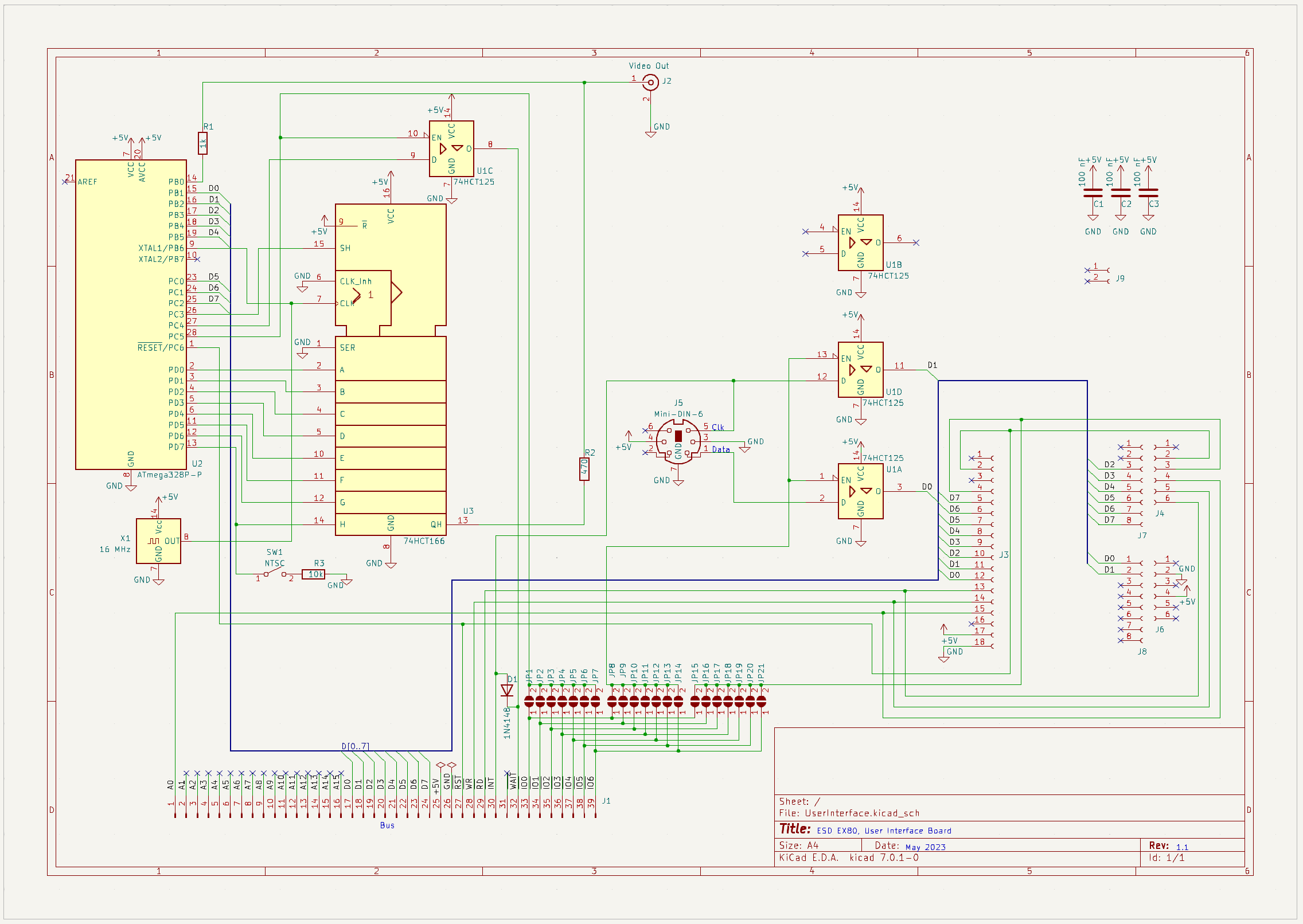
The so called i80 bus is still common in new electronics, like the cheap LCDs for Arduino you can find e.g. on eBay. Thus, this board has connectors for two different LCD form factors, e.g. the Arduino UNO one. Unfortunately, like with CF cards, some LCDs with i80 bus are not tested against a real 8080 or Z80, so timing must be a bit different. On the LCD seen in the image, I just fixed the LCD_WR line to ground and LCD_RD to +5V. Another LCD I bought on eBay works just out of the box.
The board also features a Video Out which is again similar to a design by Grant Searle, where I changed the interface from serial to the EX80 bus. To switch between TFT and external video, just press F1 or F2 at any time.
This board is also compatible to PS/2 keyboards but without utilizing a microcontroller. Here, a 74HCT125 is sufficient to read directly the Clk and Data lines from the PS/2 connector. Clk is also connected to the INT line and the system reacts fast enough to an interrupt to read the sent data bit by bit.
Floppy Controller
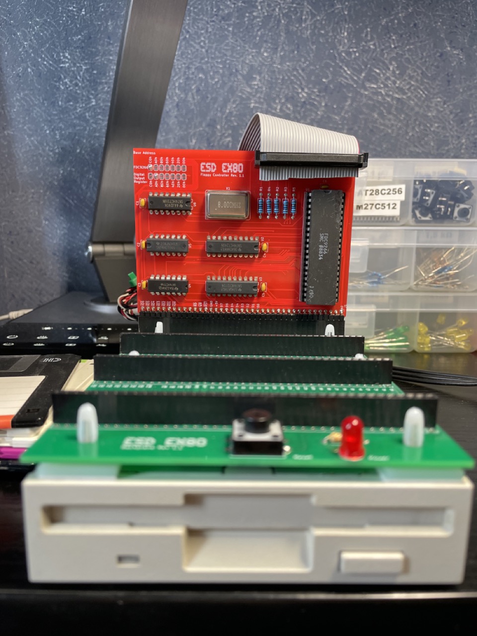
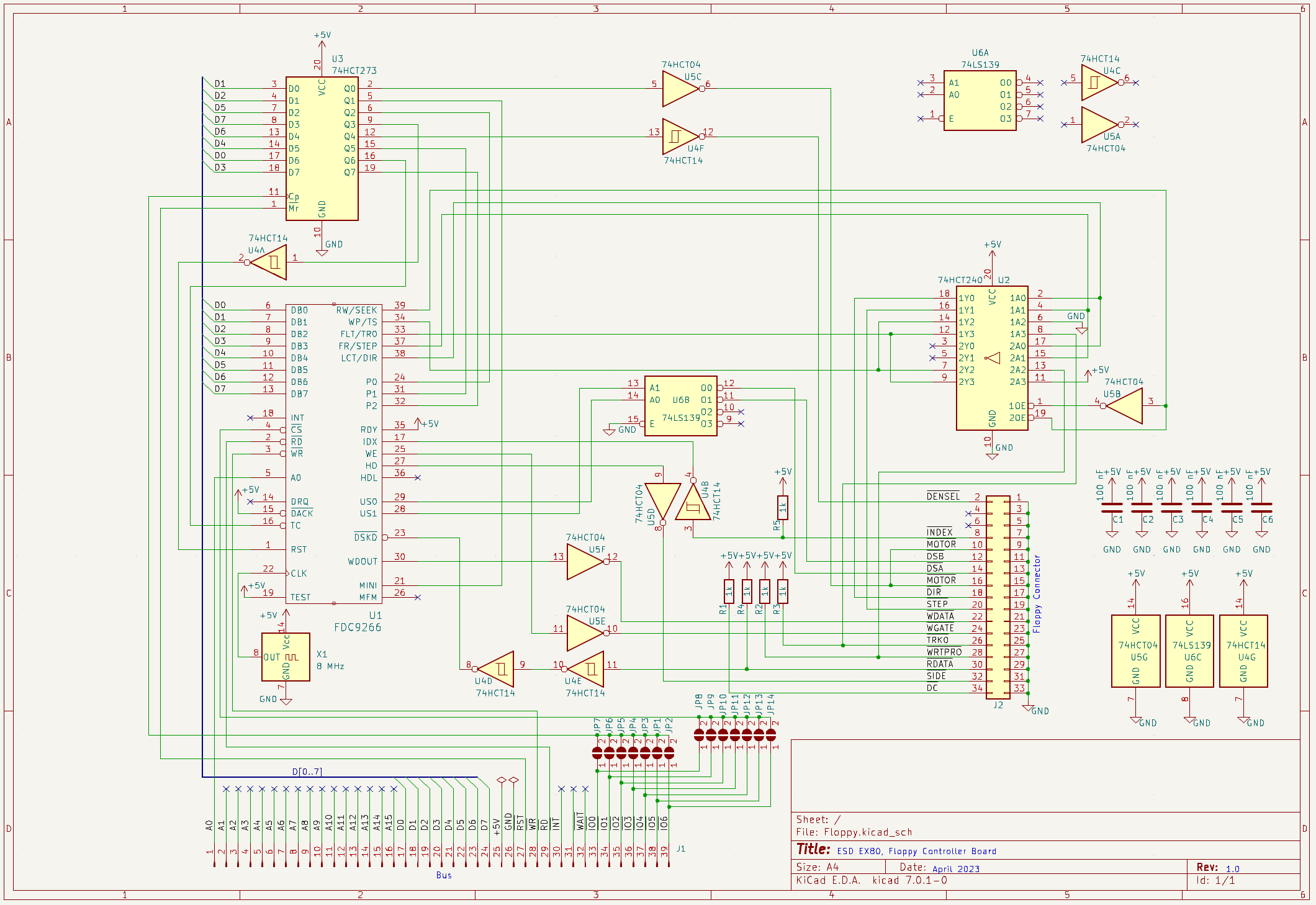
The floppy controller is based on the Zeta SBC (Aug. 2011) with modifications to plug it into to EX80 bus. This is actually all that should be mentioned.
Backplane
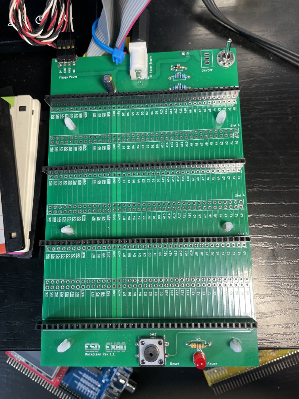
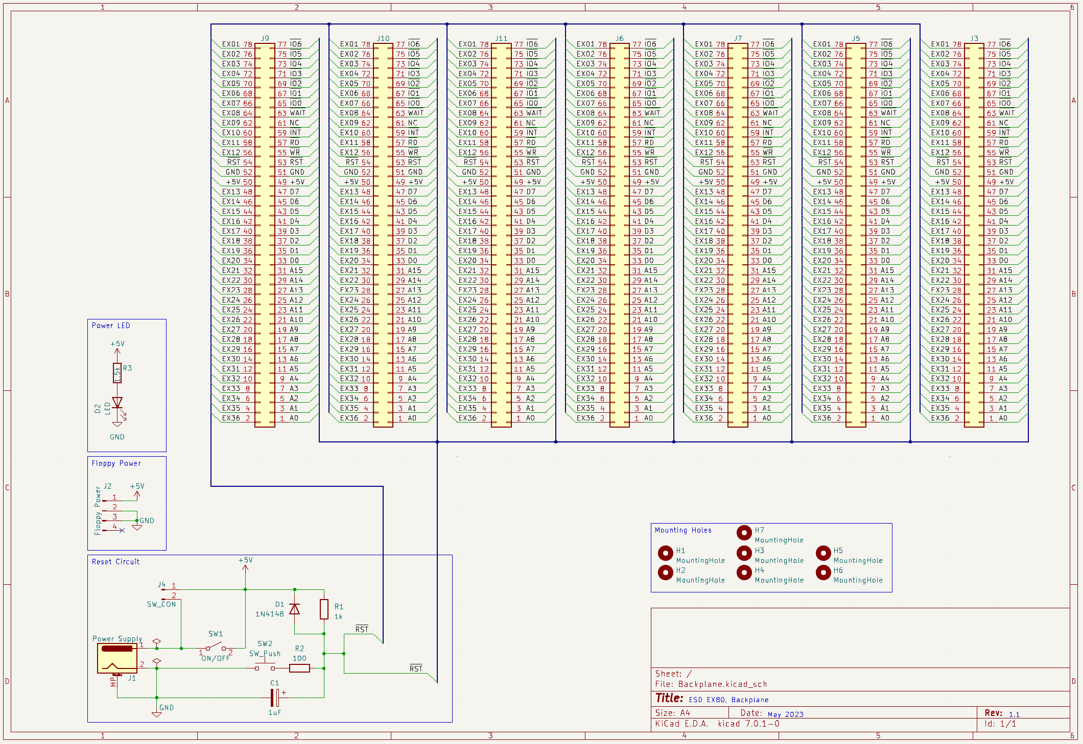
The backplane is an exception to all of the boards above as it is not based on anything 😉. As you can see, every slot has 2×39 pins, where the row towards the power connector is the processor bus and the other is the tool bus. Currently only the processor bus is populated. Don’t be confused by the bus labels. They are actually next to the utility bus but describe the processor bus.
The processor but is comparable to common buses with a few exceptions, described in the Mainboard section. The utility bus is for future expansions, e.g. to have space for SPI, I2C or other bus types that would be provided but a bridge board, that plugs into both rows in one slot. As currently there no need for this, these rows are not populated.
Furthermore, there is a reset and power on circuit, power connector for a 5V PSU, power connector for a 3.5″ device and a power switch. There are two options to mount the switch: solder it directly to the board or solder two wires and then screw the switch into the large hole.
To mount the backplane directly onto a 3.5″ floppy drive as shown in the images, there are six 4 mm holes for adhesive standoffs (LCBSB-3-01A-RT), sticked to the drive.
Firmware, CBIOS and BIOS
I don’t want to go into details about the CP/M way of BIOS, CBIOS etc., you can find very good descriptions on the web. However, this project handles some things differently and I would like to explain how. The reason for this is that it makes the boot process way simpler with the draw back that only this CP/M is supported. Further, it allows us to switch the ROM off and on during runtime to save RAM. I will now explain how this works.
If you have a look at the content of the firmware archive (see above for the download link), you will only see a a single ASM file ROM-CBIOS.asm that includes the other assembler files, including CP/M 2.2. After assembling, you will get a binary file ROM-CBIOS.bin (and listing) that covers the whole 64 kb address space of the system. In the Makefile, some dd extract the first 8 kb to a separate file (ROM.bin) that can be burnt to the EEPROM. It then contains the important drivers for floppy disk, TFT, PS/2 etc. to run the system. These drivers are quite large, but fortunately we have enough space in the ROM.
After this ROM part the binary file is actually empty before the CP/M part starts that is always at the end of RAM. Another dd in the Makefile extracts this to cbios.bin which will be written into the first two blocks of the boot floppy. Here mainly the software can be found that is expected by CP/M to be at the end of the RAM.
A bit simplified, the boot process is now the following. It starts with the ROM that just loads the first two blocks from the boot floppy into the upper RAM area. Afterwards, the ROM is switched off by setting bit 0 of the register at I/O 7 (E0h) to 1 and now CP/M continues. If the BIOS needs to access any of the drivers again, the ROM is switched on again until the BIOS code returns to CP/M.